Semiconductor Menu
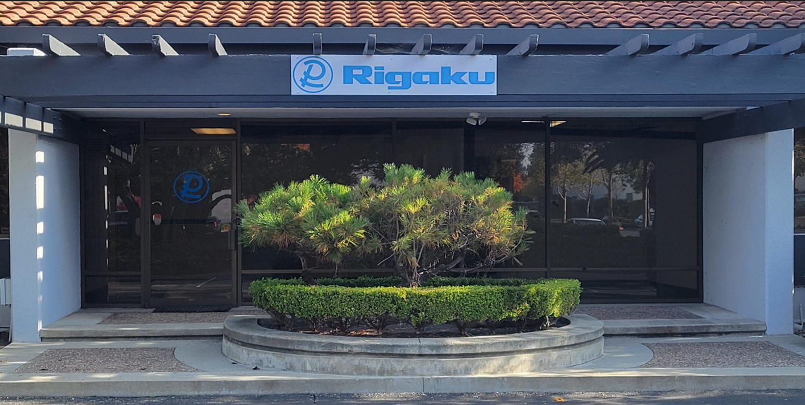
Rigaku Technology Center Silicon Valley
A technology center designed for our customers
Rigaku Corporation, along with its Semiconductor Metrology Division, is expanding its operations in Silicon Valley to improve its services for American market customers and enhance the corporation’s innovation links with US semiconductor manufacturers.
We provide demonstrations of metrology tools, offer service and applications training, and showcase the latest technologies for thin film inspection, metrology, and monitoring.

Contact Us
Whether you are interested in getting a quote, want a demo, need technical support, or simply have a question, we're here to help.